Google To Push Its Tensor Processing Unit AI Engine

Powerful AI is particularly needed for training the large neural networks that run the prediction systems and natural language processing integral to digital commerce today. Google previewed Tensor Processing Unit version 4 (TPUv4) abilities in that area last year when it bench-marked three systems in MLPerf’s v0.7 training set, which was released in July 2020.
Google may be buying heavens only knows how many GPUs to run HPC and AI workloads on its eponymous public cloud, and it may have talked recently about how it is committed to the idea of pushing the industry to innovate at the SoC level and staying out of designing its own compute engines, but the company is still building its own Tensor Processing Units, or TPUs for short, to support its TensorFlow machine learning framework and the applications it drives within Google and as a service for Google Cloud customers.
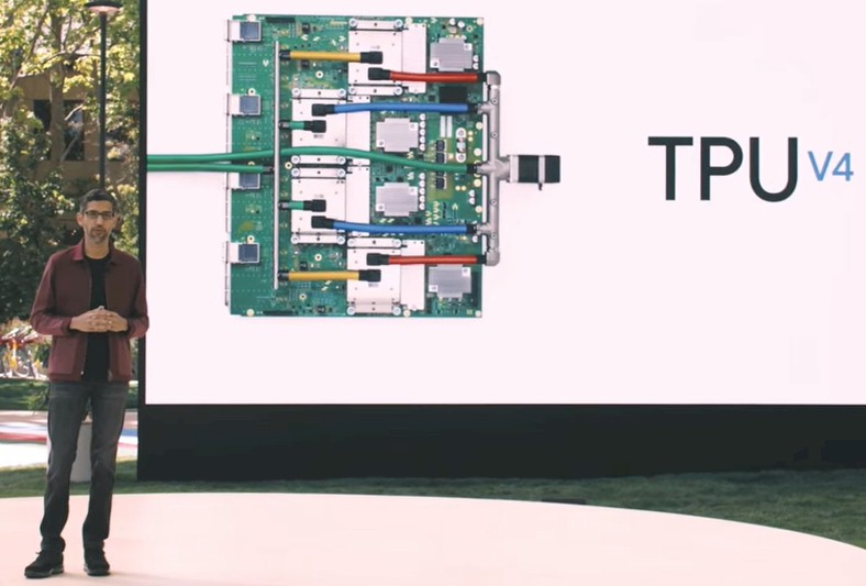
If you were expecting to get a big reveal of the TPUv4 architecture from the search engine giant and machine learning pioneer at its Google I/O 2021 conference this week, you were no doubt, like us, sorely disappointed. In his two-hour keynote address, which you can see here, Google chief executive officer Sundar Pichai, who is also CEO at Google’s parent company, Alphabet, ever so briefly talked about the forthcoming TPUv4 custom ASIC designed by Google and presumably built by Taiwan Semiconductor Manufacturing Corp like every other leading-edge compute engine on Earth. As the name suggests, the TPUv4 chip is Google’s fourth generation of machine learning Bfloat processing beasts, which it weaves together with host systems and networking to create what amounts to a custom supercomputer.
“This is the fastest system that we have ever deployed at Google – a historic milestone for us,” Pichai explained in his keynote. “Previously to get an exaflops, you needed to build a custom supercomputer. But we already have many of these deployed today. We will soon have dozens of TPUv4 pods in our datacenters, many of them which will be operating at or near 90 percent carbon-free energy. And our TPUv4 pods will be available to our cloud customers later this year. It is tremendously exciting to see this pace of innovation.”
First thing, right off the bat, no matter what Pichai says, what Google is building when it installs the TPU pods in its datacenters to run its own AI workloads and also to allow others to run theirs using Google Cloud and its AI platform stack as a service is absolutely a custom supercomputer. It is the very definition of a custom supercomputer, in fact. We certainly have our “need more coffee” days here at The Next Platform, as evidenced by the typos, broken sentences, and such, but we are running at high speed every day and we aren’t running Google with a team of speechwriters and doing a prerecorded event. Have some more coffee, Sundar. We’ll send you a Starbucks card. Have a good swig and then actually tell us about the new TPUv4 chip. (Actually, Urs Hölzle, senior vice president for technical infrastructure at Google, has promised us a briefing on TPUv4, and we are officially reminding him of that right here, right now.)
Pichai did not say very much about the about the TPUv4 architecture, but we can infer some things from what little he did say – and we won’t need a TPU ASIC to do the inference, either.
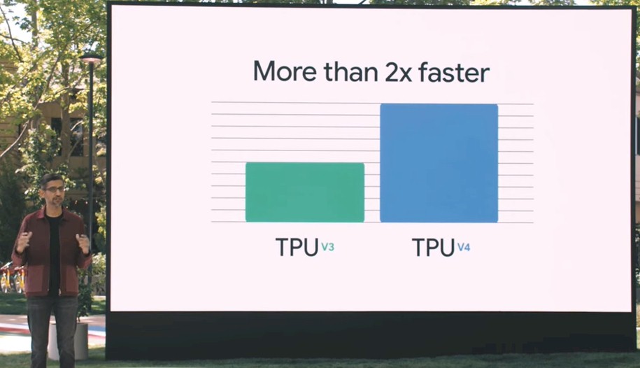
This chart literally cracked us up with its sparsity – and its weird inaccuracy unless you can infer what Pichai must have meant, which we think we have. There is such a thing as oversimplifying to the point of ridiculousness, and given that this is supposed to be the Google I/O 2021 nerdfest, we are, as we said, a little disappointed. In any event, the chart actually shows the TPUv3 having five units of performance and the TPUv4 having ten units of performance, which is precisely 2X the performance. But the label says “More than 2x faster,” which will be perplexing to some.
If this was an actual technical presentation, what Pichai might have said is that the TPUv4 has twice as many compute units running at the same clock speed thanks to a process shrink that allows each TPU socket to have twice as many compute elements – and presumably at least twice as much HBM2 memory and at least twice as much aggregate bandwidth to balance it out. But Pichai did not say any of that.
But we are, and that is what we think Google has done, in essence. And frankly, that is not that much of a stretch, technologically speaking, if that is all that Google has done to move from TPUv3 to TPUv4. Hopefully there is more. It’s a scalar/vector processor with a bunch of 128×128 Bfloat16 matrix math engines attached and some HBM2 memory.
Perhaps some review is in order and then we will tackle what the “More than 2x faster” thing might mean.
Here is a chart that sums up the prior TPUv2 and TPUv3 units and the server boards that employed them:
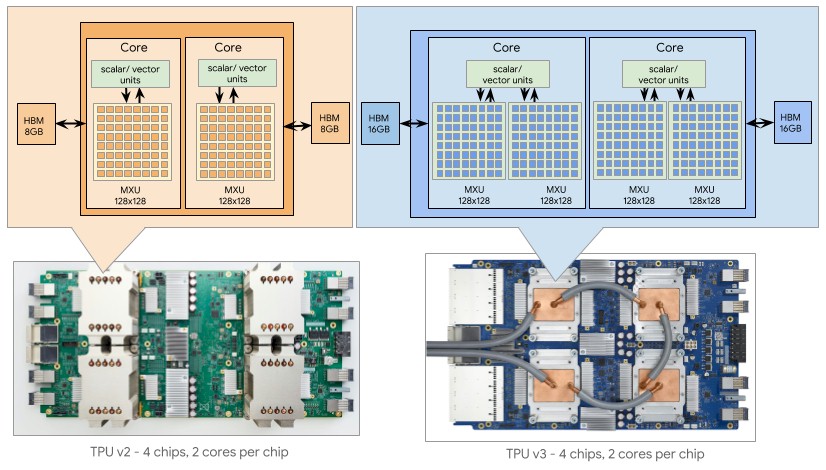
The basic TPU core is a scalar/vector unit – what we call a CPU these days given that Intel, AMD, Power, and Arm processors all have a combination of these elements – that has a Bfloat matrix math unit, which Google calls an MXU. There are two cores on a TPU chip. That MXU can process 16,384 Bfloat format floating point operations per clock, and with the TPUv2 core could drive 23 teraflops of Bfloat operations, which worked out to 46 teraflops per chip. We never did know the clock speed, but we guess it is somewhere north of 1 GHz and south of 2 GHz, just like a GPU is. Our guess for the TPUv2 is 1.37 GHz, in fact, and for the TPUv3 it is around 1.84 GHz. We dove into the TPUv2 and TPUv3 architectures here, if you want to really get into it as well as the intricacies of the Bfloat format, which is very clever, read that. The estimates for the TPUv3’s watts were way, way low. We think TPUv2 was etched in 20 nanometer processes and TPUv3 was etched in 16 nanometer or maybe 12 nanometer processes, and we are guessing that Google has done a shrink to 7 nanometers with TPUv4 and still staying in the 450 watt thermal envelope per socket that its TPUv3 pods required. We do not think there is much thermal room to raise the clock speed with TPUv4. Sorry. As it is, the increased memory might push it to 500 watts.
Anyway, with TPUv3, the process shrink allowed Google to put two MXUs against the scalar/vector unit, doubling up the raw performance per core at constant frequency; we suspect Google was able to also goose the clock speeds a little. The TPUv3 had two cores per chip, and doubled the memory up to 16 GB of HBM2 per core compared to 8 GB per core for the TPUv2 chip.
So using our handy dandy ruler and a 2X multiplier, we think Google has moved to 7 nanometers and is getting four cores on a die. It may be doing this by creating a monolithic TPUv4 die, or it may be experimenting with chiplets and created an interconnect that links two or four chiplets to each other within a socket. It really depends on how latency sensitive workloads are within a socket. Because the HBM2 memory hangs off the MXUs, as long as the MXUs all have their own HBM2 controller, we really don’t think it matters much. So if we were doing this and we wanted to increase the yield on the TPUv4 die and also decrease the cost of the chips (but pay some of that back on chiplet packaging), we would take four TPUv3 cores and break them into chiplets to make a TPUv4 socket. But it looks like Google is sticking with a monolithic design.
We would also push the thermals up as high as they can go. The TPUv2 weighed in at 280 watts and the TPUv3 cranked that way up to 450 watts to drive 123 teraflops of performance. (Implying a 33.7 percent boost in clock speed moving from TPUv2 to TPUv3, but paying for it with a 60.7 percent increase in power from 280 watts to 450 watts.)
We think the HBM memory on the TPUv4 device doubled, but the HBM2 memory per core could be the same at 16 GB per core. That would be 64 GB per device, and that is a lot. (Yes, we know Nvidia can do 80 GB per device.) There is an outside chance that Google might push this as far as 128 GB per device, or 32 GB per core. That really depends on thermals and cost. But what we do know for sure is that Google and other AI researchers sure do wish more HBM2 memory was available on these devices. We think it is highly unlikely that the clock speed on the TPUv4 device will rise much. Who wants a 600 watt part?
Now, let’s talk about that “More than 2x faster” comment above. Last July, Google put out some early data comparing TPUv4 performance on the MLPerf suite of AI benchmarks to the TPUv3 devices. Take a look:
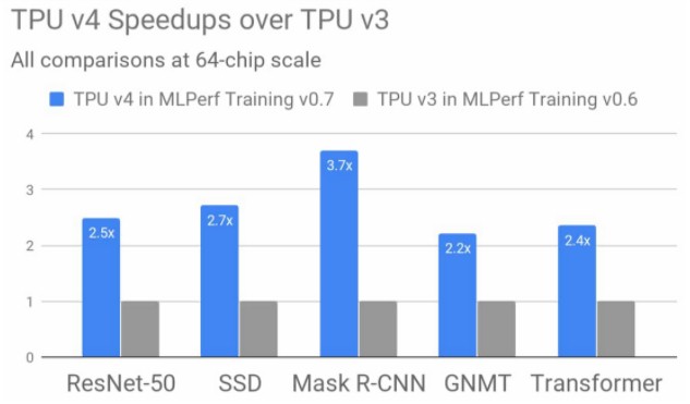
On various components of the MLPerf machine learning training benchmarks, the performance increase moving from TPUv3 machines with 64 chips (128 cores) to TPUv4 machines also with 64 chips (and 128 cores) ranged from 2.2X to 3.7X, and averaged around 2.7X for these five tests. So that might be the “More than 2x faster” that Pichai is talking about. But that is not what his chart showed. The difference between the 2X hardware peak performance capacity and the 2.7X average increase in MLPerf performance is – you guessed it – software optimization.
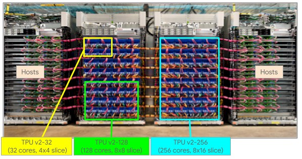
The TPU pods get carved up virtually in the following fashion. Here’s the TPUv2 pod:
And here’s the TPUv3 pod:
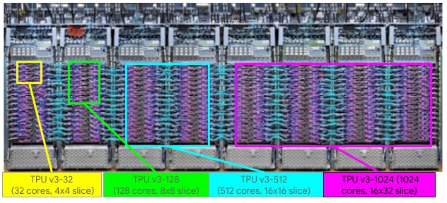
The largest TPUv2 image was 512 cores and 4 TB of HBM2 memory and the largest TPUv3 image was 2,048 cores and 32 TB of memory.
Now, Pichai said that the TPUv4 pod would have “4,096 chips” and assuming he didn’t mean cores, that could mean that it has 4,096 sockets and each socket has a monolithic chip. That fits what Pichai said and gets the TPUv4 pod to just over 1 exaflops at Bfloat16 precision. (The TPUv2 pod could only scale to 256 chips and 11.8 petaflops and the TPUv3 pod could only scale to 1,024 chips and 125.9 petaflops, by comparison.) That 1 exaflops assumes the clock speeds and thermals for the TPUv4 socket are roughly the same as the TPUv3 socket and Google is quadrupling the socket count.
We also think the TPU instance will be able to scale across all of those 4,096 chips and sockets in a single system image, with at least 64 TB of aggregated HBM2 memory. And thanks to the software improvements, more of that peak will be driving the workloads. We shall see how much when Google actually tells us more.
One last thing: Pichai also said that the TPUv4 pod had “10X the interconnect bandwidth per chip at scale compared to any other networking technology.” In looking at the TPUv4 server card compared to the TPUv3 card in the diagrams above, it looks like each TPUv4 socket has its own network interface; the TPUv3 card had four sockets sharing two interconnects. (Or, it looks like that. We are not certain this is correct. Those could be two-port router chips.) We look forward to learning more about the TPUv4 interconnect.
Adblock test (Why?)
Staff writer. Jonas has an extensive background in AI, Jonas covers cloud computing, big data, and distributed computing. He is also interested in the intersection of these areas with security and privacy. As an ardent gamer reporting on the latest cross platform innovations and releases comes as second nature.